|
In the introductory article, I showed how to set up Gus Smalley's Beginner
Boost V. 2 with tone stack on a solderless breadboard. Now we will commit to a soldered build on perfboard
and house the effect in a gig-worthy enclosure. If you bought one of the breadboarding kits, the parts can be re-used
if you wish. The result will be a professionally-useful pedal with all of the
features that you would expect of a commercially-manufactured "boutique" design.
As I have done with some of my other "Breadboard-To-Box" projects, I will
describe some of the electronic and mechanical considerations that went into
developing the finished design. If you are new to building pedals, you'll
learn some good construction habits and patterns of thinking and planning that
will be helpful in building more complex designs.
I'll show two possible builds: The generic build on the right uses a
standard 125-B enclosure that is available from many sources. On the left
is a "deluxe" build in the made-for-Small Bear Bare Box #1. That one uses a
number of made-to-order parts and specific modular connectors to produce a
result that is comparable to a manufactured product. The sloped design
reduces greatly the risk of stomped pots, and it includes a battery door.
The difficulty levels of both builds are about the same, and complete
kits are available to take you either way. |
|
  |
|
|
|
|
Breadboard To Box - What Is Involved?
If you followed the breadboard build to its end, you have a working circuit, complete from input to output, like
Figure 1.
Clearly, a number of elements need to be added to make this into
a buildable design for a finished pedal. The most important is bypass switching, to allow the effect to
be foot-switched in and out. There are numerous schemes for doing this, and I
chose one that's known to work well and uses components that can be found almost
anywhere.
|
|
 |
|
3PDT True-Bypass Switching With In-Use LED Driver - How It
Works
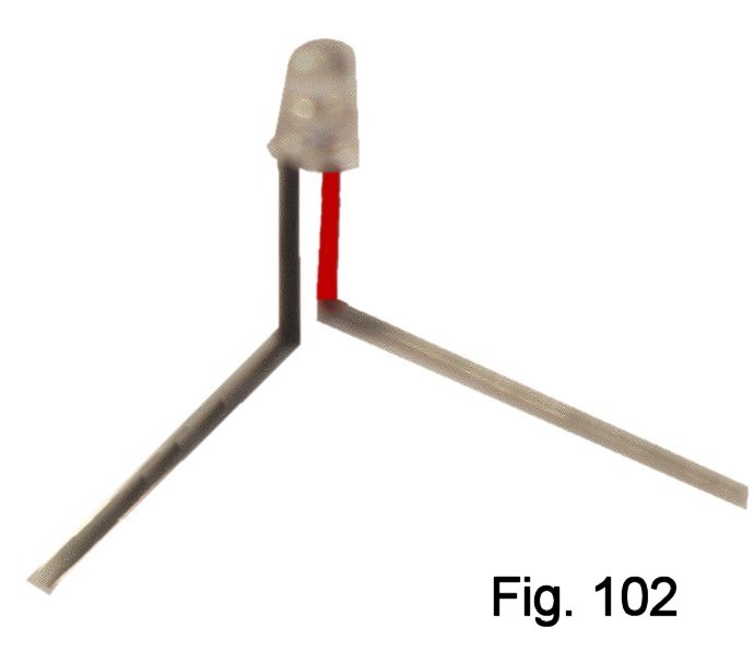
Here's a bottom view of a typical 3PDT (Three-pole,
Double-throw) footswitch. It has nine contacts, and they work as shown in the schem
in Figure 2. Push/release once and the moving contacts (2, 5 and 8) connect to #3, #6
and #9. Push/release again
and they go back. We call this a "latching" or "alternate-action" switch,
because the contacts remain in their new positions when you release the switch.
|
|
 |
|
Let's add this to the schematic, trace through the connections and see how
the switching works in practice. In Figure 3, the effect is
bypassed. The guitar input goes from the moving contact, pin 2, through
stationary contacts pin 1 and pin 4 (which are connected with a jumper) to
moving contact pin 5 and then to the output jack When the switch is stomped,
the input jack sees the effect input through pin 3, and the output jack sees
the tone
control through pin 6. Two contacts of the third pole switch the LED on and
off. OK so far? If you still have the circuit on your breadboard and want to set
up the bypass to see/hear it work, by all means do so.
Answer to a FAQ: There are other ways to wire a stomp switch,
with and without an in-use LED. They will all work, though some may be more
suitable than others in a particular design situation. If you want more
information, check the Beginner FAQ or other on-line sources.
|
|
 \ \ |
|
Power - Internal and External
While we were on the breadboard, we switched power off by
disconnecting the battery. That won't work in a pedal, so we have to make some
arrangements. And there are several issues:
-
We want a DC power jack, and we want the battery to be cut off when an external power supply is plugged in.
-
We want the circuit to be protected from reverse connection of
power.
-
We want battery power to be cut off when the guitar plug is
removed from the input jack.
Most modern pedals accomplish all of this in the same ways.
External power comes in through a jack like the one of the ones in Fig. 4. These styles
are designed to be mounted on the panel of an enclosure, while others mount on
a circuit board. They all work similarly, as shown in the small schematic
(Fig. 5).
Contact #1 connects to the shell of the power plug, which will be positive in the
typical negative-ground pedal design. Contact #3 forms a normally-closed switch
with contact #1; it shorts to #1 until a power plug is inserted. Contact #2 is
the center pin, which will be ground in this configuration. |
|

|
|
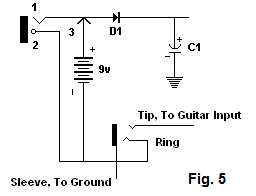
Switching the battery off when the guitar is unplugged is done by using a stereo
jack for the input. Since the Ring contact of such a jack is shorted to ground
through the sleeve of a guitar plug, it provides a cheap and easy way to
implement a necessary function. Do take a look at the physical jack and work out
for yourself what is happening if you need to. Figure 5 shows the whole idea in
schematic form. Diode D1 takes care of reverse polarity protection; it will block current flow
if the battery or power supply is connected incorrectly. |
|
 |
|
|
|
Here is the whole, buildable schem, including all of the support circuitry.

|
|
The "Bare Bones" Of Planning A Build |
|
|
|
When working out a design, the first job is to translate the schematic to a
suitable layout on a chassis or circuit board. You may notice that the
layouts of many "Build Your Own Pedal" articles are pretty ad-hoc and
haphazard. I organize my builds by following a rule that I worked out from
listening to some of the
engineers on the Forum, especially R. G. Keen: "Pick a suitable enclosure,
then figure out where the off-board components will go, and then lay out the
board so that the connections to the off-board components are as direct as
possible." |
|
|
|
I know that this will be a two-knob build, so I will want
terminations for:
- Two potentiometers
- DC Power
- Input from guitar
- Output to amp
- Stomp Switch
- In-Use LED
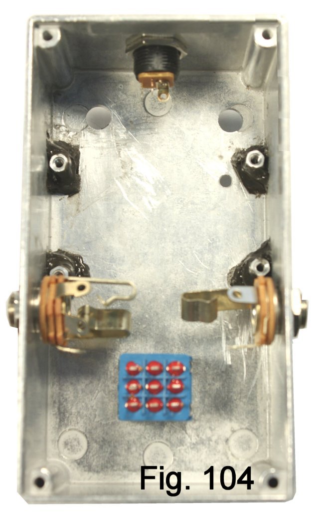
I've already chosen a rectangular enclosure, oriented vertically like a
typical off-the-shelf pedal. Putting the input jack on the right has become
an industry standard, the stomp switch logically goes at the bottom and the
power jack and pots at the top. Where the LED goes is a matter of taste; I
usually locate it on the top left side.
This defines the basic layout of the enclosure, and we can now think
about laying out the circuit board. When looking at the top of the case, the
board inside actually sits component-side down, right?. So, turning the case
over gives our first look at where the off-board terminations will be (Fig. 8). |
 
|
|
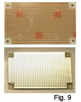
FAQ: Which Material? Pad-Per-Hole vs. Veroboard You will
see many designs laid out on stripboard, also called Veroboard, or just Vero
(Fig. 9). While I stock it because it's very popular, I don't recommend it for first
builds. It's very convenient to use, but it does not force you to follow the
logic of a schematic and wire point-to-point. To my mind, that's an
essential skill that a beginner needs to develop.
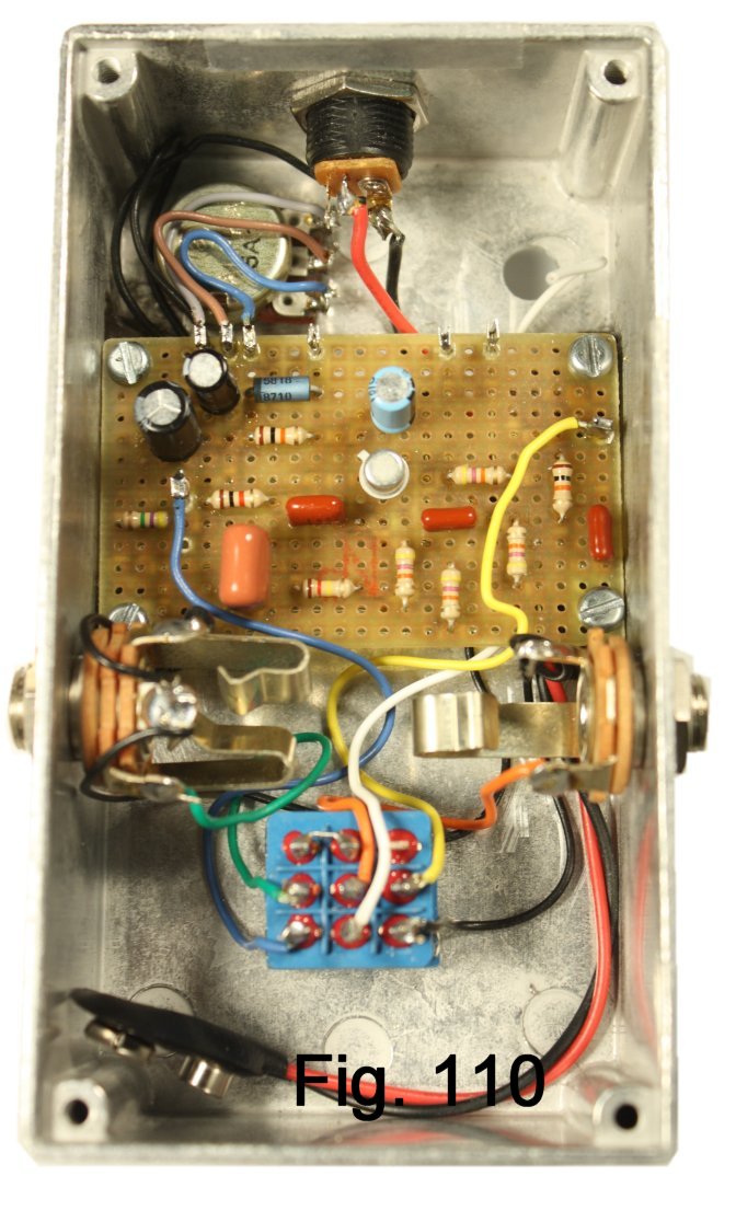
I recommend perforated
circuit board, or perfboard as it is commonly called (Fig. 10). Each hole on the
bottom of the board is surrounded by a tinned copper
pad to which solder can bond. This type of stock is called, appropriately,
pad-per-hole perfboard. Component leads are inserted through the holes and
soldered in place on the opposite side. Connections are made with short lengths
of bare wire.
|
|
  |
|
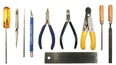
Tools and Materials Some DIY builds are entirely
paint-by-number, which I don't like--they don't teach much. Both builds in this
article
include some hand tooling. Before you begin creating the board, let's make sure that you have all the tools
required. You'll need a few basics:
- 25- to 35-watt soldering iron, rosin-core solder and cleaning sponge
- Small screwdriver(s)
- Small chain-nose pliers and side-cutters
- Small locking-grip ("Vise-grip") plier
- X-acto or similar knife
- Self-locking tweezers or other "third hand"
- Small alligator clip
- Colored pencil or "Hi-liter" felt-tip marker
- Some small round and flat files
- A pointed steel "pick" or scratch awl
- De-soldering braid
If you buy one of my kits, case is pre-drilled. If you are
rolling-your-own, be prepared to borrow
a drill if you don't have one.
|
|
For finishing the case you'll need:
- 220-grit and 400- (or finer) grit carborundum paper
- Acetone, denatured alcohol
- Spray primer and enamel
- Decal stock or decals
- Clear lacquer like Krylon
These tools, and many others, are available in my Stock List.
|
|
|
|
|
|
First Job - Tool The Perfboard |
|
Here is how to tool the 60 x 60 board
for both the generic and the Bare Box builds. However, the methods are similar if you are using
locally purchased material of any larger size. The drawings below (Figure
11) show what we need to wind up with.
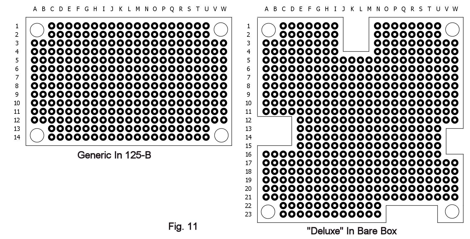
For the generic build, the 60 x 60 needs to be cut down to 14 rows and
two mounting holes must be added. If you don't have a Dremel tool, use a
knife and a steel rule to score
the board in the 15th row all the way across (Figure 12). Score a dozen or so times in
order to deepen the line. If you have a vise or have access to one, clamp
the piece in the jaws on the score line. Wedging the piece in a door frame will
also work (Figure 13). Apply steady pressure on the edge until you feel the
material snap. Borrow a drill if necessary to create two new 1/8" mounting
holes (Figure 14).
  
If you have a Dremel tool
and an abrasive cutoff wheel, this combination is by far the easiest way to
work perfboard. However, if you go this route, be aware that the dust that
the operation throws off contains fiberglass.
WEAR GLOVES, GOGGLES AND A
FACE MASK!
|
|
|
|
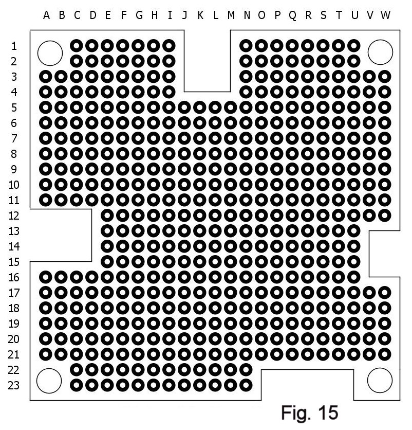
The 60 x 60 is exactly sized for the Bare Box, but it needs four cutouts to
pass wiring from the off-board components. The coordinates are shown in
figure 15. Using a knife, mark the outlines of the areas that need to be cut away (Fig. 16).
|
|
If you are limited to manual tools, continue using the knife and score each line
that you have marked a dozen times. Then use pliers to bend and snap on the
score lines, "nibbling" a little at a time (Fig. 17). Clean up the
edges with a flat file (Fig. 18) and you should wind up with a piece that looks
like figure 19. 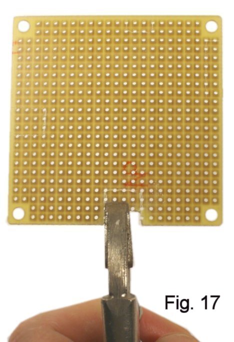  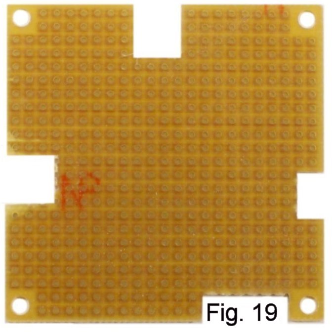
|
|
|
|
Short Answer To An FAQ: How Do You Get To A Workable Component Layout? |
|
The long answer really needs another tutorial by someone who has designed
boards for a
living, like R. G. Keen. In
his case, he wrote a book.
Short answer: We know where the off-board connections will be, so figuring out
exactly where each component will go needs a lot of
place-and-try. I see many attempts to use pencil-and-paper for this process,
and I always advise against it; there are numerous software packages--some
free to download--that make laying out a board both a lot easier and fun. Like all
programs, they have a learning curve. But if you invest the time, you'll be
amazed at what you can do going forward. I use DIY Layout Creator, which can
be downloaded from a link on the Forum. If you are building in the Bare Box, continue in the next section. For
the generic build continue below.
|
|
|
|
|
|
Stuffing The Board For The Bare Box Below is the
board layout and a re-cap of the parts list. You are seeing the board
in "X-Ray" view; the red lines are connections that we will make with bare
wire on the bottom of the board.
Print a copy of this drawing and the schematic so that you can mark off connections with a
highlighter as you work. This is one of my time-tested methods for catching
mistakes before they cost me time and frustration.

|
| R1 |
4.7 Meg |
| R2 |
1K |
| R3 |
120K |
| R4, R5, R8, R10 |
47K |
| R6 |
10K |
| C1 |
100 mf. |
| C2, C6, C7 |
.01 mf. |
| C3 |
.47 mf. |
| C4 |
22 mf. |
| C5 |
1 mf. |
| Q1 |
2N2222A or similar |
| D1 |
1N5818 |
|
|
|
|
We are ready to populate
("stuff") the board. While components can be added in any order,
I'm going to suggest that you start by installing the Molex headers for
power, signals, switching and the pots. With those in place, you'll have good physical
reference points for installing all of the other parts. Please note that I don't
cover basic soldering techniques in this article; you may want to check a
reference and do some practicing if this is your first build.
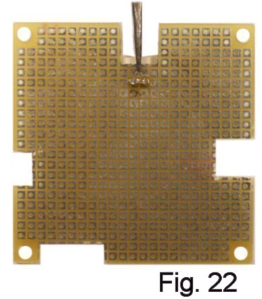
Find one of the
two-pin horizontal Molex headers (Fig. 21). Install with its pins in indexes
K-6 and L-6, use self-locking tweezers to hold it and solder in place
(Fig. 22).
In the same way, locate, install and solder in place the other horizontal Molex
headers: three-pin for the input, two-pin for the output and six-pin for the
stomp switch. Follow with the two three-pin vertical headers for the
potentiometers (Fig. 23, Fig. 24). Align the vertical headers as shown in the pic with their chamfered sides to the left.
   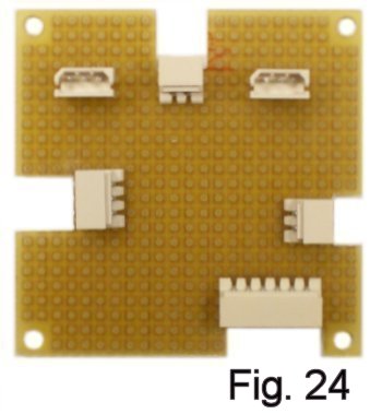
We are ready to add components. |
|
|
|
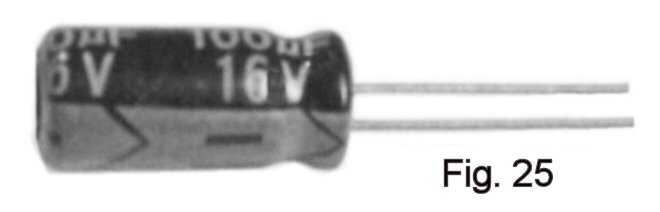
Install the 100 mf. electrolytic capacitor (Fig. 25) with its positive side
in index F-2. Solder in place and trim leads on the bottom (Fig. 26). Save
those scraps of bare wire for later use in making connections!
|
|
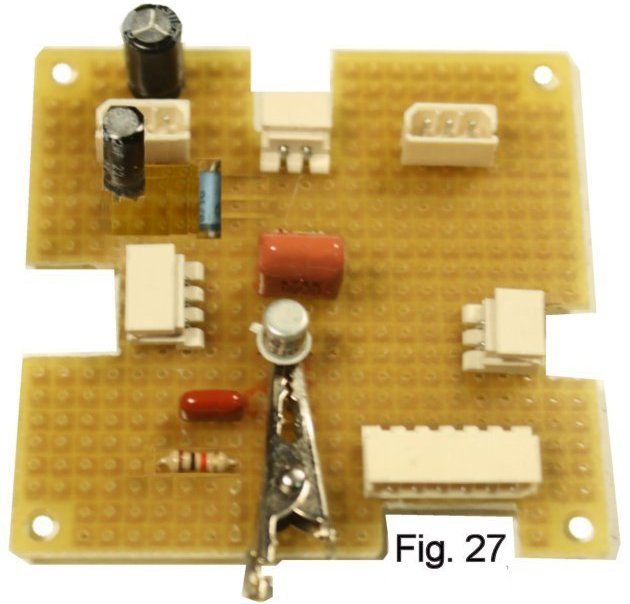
Keep adding components, working up-and down and left to right.
Capacitor C3 may span three, four or five holes depending on the make,
so form its leads accordingly. Observe
polarity for the electrolytic capacitors C4 and C5. While silicon transistors and diodes are not
as heat-sensitive as their germanium counterparts, it is a good idea to use
an alligator clip as a heat sink, putting it on each lead of the device
before soldering as in figure 27. Figure 28 shows the
board fully populated except for the LED. That goes in last, during final
assembly. When planning a board layout for manufacture as a printed circuit board,
jumpers are sometimes a way to avoid the expense of a double-sided PCB. The
two jumpers on the component side are shown as thin blue lines in the
layout drawing. They can be formed from the scraps of wire that you trimmed
from the other components, or you can use the tinned bare copper wire in the
kit. Form a jumper that spans seven holes, install in indexes M-18 through
S-18, and solder in place. The second jumper connects indices Q-14 and Q-16.
Figure 29 shows both jumpers in place. |
|
|
|
   |
|
|
|
|
Wiring The Board Now for the plumbing! With all the components in place, we begin to make
connections between them with short lengths of bare tinned wire. First we'll
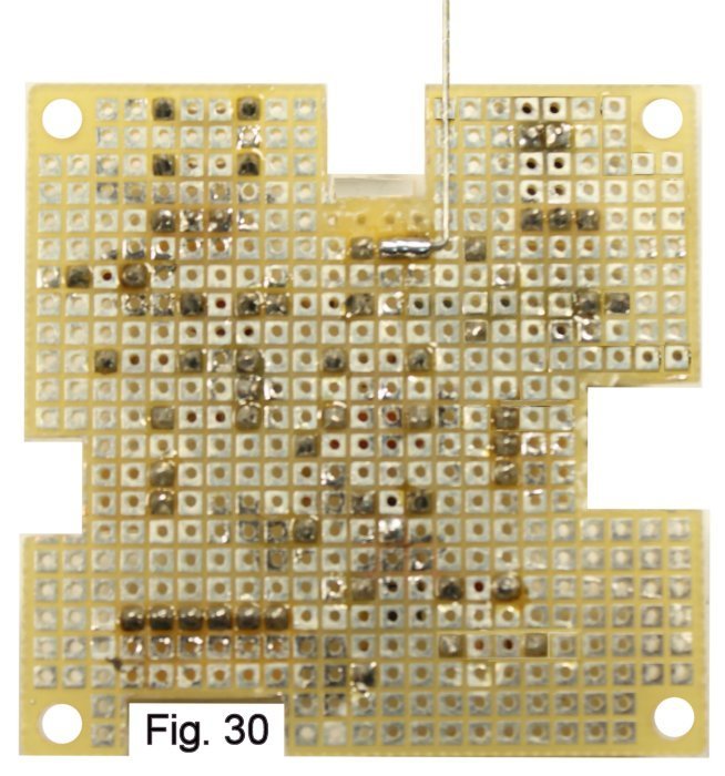
do a long one: from the negative power input to the Ring of the input jack
J2. As shown in figure 30, butt a length of bare wire up to index K-6. Use the
locking tweezers to hold it in place and solder at K-5/K-6. Now use a
chain-nose plier to put a right-angle bend in the wire. Make this as sharp
as you can, and centered in column I. "Tack" this part of the run with a
little bit of solder at index I-1, bend downward in column C and tack again at index
C-1. Bend clear of the mounting hole to get over to column A Bend downward,
right-angle bend again at A-11 and tack at B-11. 45 degree bend at D-11 and end at G-12
(Fig.31). If you want your best shot at
having the build work right off the rip and you have a multimeter, use the
continuity function every time you solder a connection to make sure that the
points you think are connected Really Are. The terminals of the connectors
Are accessible from the top of the board (Fig. 32).
   . |
|
|
|
Now try the ground run that starts at the negative side of electrolytic
capacitor C1. Put a very short right-angle bend in the end of a length of
bare wire (Fig. 33). Insert the end into the hole at index D-2. Hold
this in place
with soldering tweezers (Fig. 34) and solder to join with the negative side
of the capacitor at pad E-2. Cut the wire just short of the pad for the
potentiometer connector at index D-5 and solder to join (Fig. 35). Butt the
remaining bare wire against the joint that you just made at index D-5, hold
in place with soldering tweezers and solder (Fig. 36).
   
|
|
Create a right-angle bend down in column 2 and another in row 8. Cut at the
negative side of electrolytic capacitor C4, index C-8. Hold the wire down
with the tweezers and solder (Fig. 37). Before continuing the run, I used the tip of my
soldering iron to remove the pads at indices G-8 and F-9. It's a way to
avoid problems where I think there might be a danger of a short between
connections. Then I set up a short right-angle bend, installed that in
index B-9 and soldered to join to B-8. This starts the rest of the ground
run as shown in Figure 38. Note that it continues after the long jumper and
ends up at R10. When finished, it is very important to test continuity all
along the run and from beginning to end (Fig. 39).
|
|
|
|
Make the connection between L-5, the positive power input, and H-6, the
positive side of diode D1. Follow with the run that connects F-2 (the
positive side of capacitor C1), H-9, (the cathode of diode D1), resistor R3
and resistor R6 (Fig. 40). I am a big fan of using the capacitance scale
found on many multimeters to test continuity where a capacitor contacts a
run on the board. Look at the layout for a second: The positive side of C1
contacts three points that are accessible on the component side, and its
negative side is grounded. So we
should see the value of the capacitor between any of those points and any
point on the ground bus, right? And so we do, as in figure 41. (The
capacitor is nominally 100 mf., but tolerance is typically 20%, so this is
in range). Used consistently, this technique will smoke out numerous joints that
are not quite connected. |
 
|
|
|
|
If you are with me so far, you have the basics of the technique. Here is a table of the rest of the connections in the order I
did them, with some notes where appropriate. With a highlighter, mark off
connections on the layout as you make them. |
The last step is actually installing the LED. For reasons you'll
see later, I leave this until after the board is tested and we know that the
effect works. Now, we can prepare the off-board components to connect to the
board and then do an initial test (!).
|
Assembling The Pots, Jacks and Switch If you
bought the breadboard kit and are re-using parts, unsolder the connecting
wires from the potentiometer terminals. I will presume here that you are
using my modular approach to making the connections, so find six terminated
leads and two male three-pin Molex housings (Fig. 42). Reserve the red and
black leads for power. Other than that, it's your choice for which
color goes where.
Install each lead into
its hole in the housing. The terminal has a flange on one side, and you will
feel it click into place when it is fully inserted (Fig. 43). Cut the leads
down to about 2", strip, and solder as shown to create the potentiometer
assemblies shown in figure 44. Take special care to get each pot on the
proper side and the terminal assignments correct.
In the same way that you created the connectors for the pots, install
black and red leads to set up a connector for power (Fig. 45).
  

|
|
Find a two-pin and a three-pin Molex plug. Assemble the connectors for input
and output, using black leads where shown in figure 46. While the other
leads can be any color, you may want to follow my example to avoid
confusion. The Bare Box #1 enclosure is tooled to be friendly to shrouded jacks like
those used in many "name" pedals. These have a chamfer (bevel) on the sleeve pin
edge, which is helpful for identifying the contacts.
Start by locating the sleeve contact of the
input jack and soldering the black center lead of the plug to this contact.
The sleeve contact is the one on the beveled edge (“chamfer”) of the jack.
For ease of assembly later, it’s best if the lead enters from the bottom of
the contact and is bent at right-angles as shown before soldering (Fig.47).
 
|
|
The last piece of pre-assembly before you put everything
together is creating the connector for the stomp switch and soldering those
components together.Find the six-position Molex connector and the terminated
leads for it, and assemble this as you did the others. While there is no
standard for which color goes in which position, you may want to follow what
I show in figure 48 for ease of troubleshooting.
Position the stomp switch with its terminals parallel to you
as shown in the left-hand pic. Start the wiring by connecting the two
terminals at the top left with a very short piece of bare wire, and then
solder. When making the solder terminations to the switch, take care to
route and dress the leads as shown; it’s important to being able to position
them in the case later. The right-hand pic is annotated to show which
termination goes to which contact (Fig. 49).
 
|
|
Initial Testing
Are you ready to test your work? Plug in pots, jacks and stomp
switch as shown in figure 50. Set both controls to their mid-points. Connect
your guitar and an amplifier and connect a battery to the power leads. If
you don't get boost, click the stomp switch. Got boost?, Tone control works?
CONGRATULATIONS!

If your build doesn't work yet, don't be too discouraged. Take a shower and grab
a bite, since we know that you haven't done either one since you started
this thing; troubleshooting requires a clear head and normal blood-sugar
level. The first rule to keep in mind is that projects like this are
all-or-nothing. If EVERYTHING is correct, the build works; if ONE thing is
wrong, it doesn't. But you have something going for you: I built from the
drawings shown here, and you can rely on them. Use them as your bible, and
you'll find out what's wrong.
To start troubleshooting, make clean copies of both the schematic and the
layout drawing. Use a highlighter to mark off connections as you check them.
Go over the off-board connections first. If those look good, you have to
verify the interconnections. Use the continuity setting of your multimeter
to make sure that you actually have a connection between every point in the
layout that is supposed to be connected, and that nothing is shorted. Found
a bug? Time to do repairs.
You can also use the low-voltage scale of your meter to sniff out
problems. With your guitar plugged in (necessary so that the battery
circuit is complete), hang the negative lead on the sleeve of the input
jack. You should see roughly the following voltages on Q1: Collector 5.48
volts, Base 2.39 volts, Emitter 1.77 volts. If any of your readings are off
these by more than 10%, you probably have a wiring error. Once everything
works, you can add the in-use LED and then proceed to the section on
finishing the enclosure. |
|
|
|
Installing The LED An LED is a diode, and so is polarized.
By convention, they are supplied with the negative lead shorter than the
positive. Insulate the leads using short pieces of spaghetti tubing, and
then bend the ends away from each other (Fig. 51).
Solder the leads to the pads on the underside of the board. Positive goes to
U-4 and negative to V-4 (Fig. 52).
Before you go further, re-assemble your test setup and make sure that the
LED works properly. If it does, the board is finished.
 
|
|
Finishing The Enclosure |
|
|
|
All the finishing methods I am familiar with begin with sanding to produce a
smooth finish that will be friendly to paint, powder-coating and/or decals.
I like to wet-sand starting with 220 grit Carborundum paper, and I use progressively
finer grits up to 600 to get a smooth finish.
You can get ideas and techniques for decorating and labeling from many
on-line sources as well as some of the other project articles at SBE. After
decorating, I always put a soft cloth down on my bench so that there is less
chance of ruining a paint job. Move slowly, especially when you have a tool
in your hands! |
|
|
|
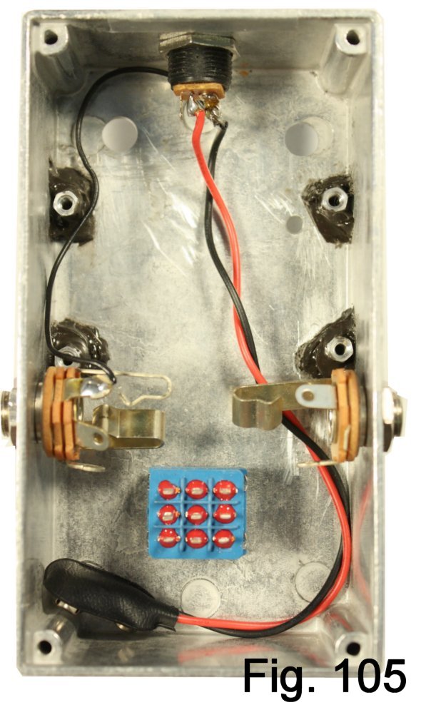
Final Assembly The next step is to wire and install the DC power jack, the
male power connector and the battery snap. Begin by slipping a ¾” length of
heat-shrink tubing onto the positive battery snap lead. Crimp the lead to
the terminal on the jack, solder, and then conform the tubing to the
connection using the side of your soldering iron.
In a similar way, attach the positive power connector lead.
The negative leads for the battery snap and the power connector go to the
ground terminal, and no insulation is needed (Fig. 53).
Before installing the assembly, thin down the shoulders of
the insulating washers so that they will allow the washers to “grab”
properly and not let the jack rotate. This can be done with sandpaper, or a
grinding stone on a Dremel tool is ideal, if you have one (Fig. 54).
The potentiometers have anti-rotation tabs that need to be cut or bent off
(Fig. 55).
  
|
|
Mount the power jack assembly first, then the pots. Take care to get the
correct pot on each side. All hardware should only
be finger-tight for now. Mount the input and output jacks, dressing
the leads as shown to keep the plugs out of the way of the stomp switch
(Fig. 56).
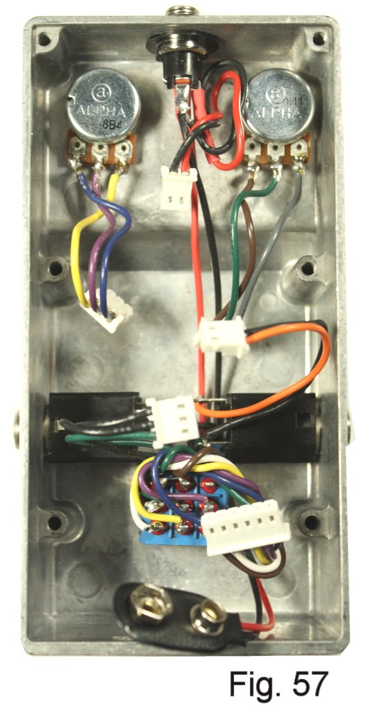
Mount the stomp switch, being sure to orient it so that the plug assembly is on the right. The battery snap leads go between the jacks
and around the stomp switch (Fig. 57). Move the plugs aside enough to ease
the board into place (Fig. 58). Plug in all of the connectors. Maneuver the LED into its mounting hole and
set
the board down on its standoffs. Install one of the round-head screws to
hold the board down temporarily. Connect your gear and a battery (Fig. 59).
|
|
Test the pedal. If something does not
work, first make sure that all of the plugs are fully inserted and that none
of the pins on the wires have worked loose. It's also possible that a
connection broke during assembly or something is shorting inside. You may
have to disassemble and go back to the troubleshooting section above.
Once everything works, finish
securing the board. The threaded studs secure the side of the board that is
next to the battery, and two of the screws that secure the lid will screw
into them. To complete the job:
- Tighten the hardware on the controls and jacks
- Secure the lid
- Stuff a small piece of foam padding over the battery
- Install the battery cover
- Install knobs
- Install rubber feet
|
|
Enjoy your new pedal! More builds employing the modular approach of the Bare
Box #1 are under development. Comments and suggestions are welcome at
smallbearelec@ix.netcom.com. |
|
|
|
A Parts List |
|
|
|
Presuming that you have all the parts in the breadboard kit, here's what's
needed for the build in the Bare Box #1: |
|
|
|
1 |
Bare Box #1 (with 6 screws and
2 studs) |
0350 |
|
1 |
DC Power Jack - Long Bushing |
0612D |
|
1 |
3PDT stomp switch |
0200 |
|
2 |
Knobs for 1/4" shaft |
0825C |
|
2 |
Molex 3-pin vertical headers |
0614S |
|
3 |
Molex 3-pin plugs |
0614U-2 |
|
2 |
Molex 2-pin plugs |
0614U-1 |
|
2 |
Molex 2-pin horizontal headers |
0614R-1 |
|
1 |
Molex 3-pin horizontal header |
0614S-1 |
|
1 |
Molex 6-pin horizontal header |
0614T-1 |
|
1 |
Molex 6-pin plug |
0614U-3 |
|
19 |
Terminated leads |
0614O |
|
1 |
Pad-per-hole perfboard |
0355 |
|
1 |
Bare tinned wire |
0509 |
A kit that includes everything on this list is available as SKU 0016C. |
|
|
|
|
|
Stuffing The Board For The Generic Build |
|
|
|
|
|
Below are the board layout and a re-cap of the parts list. You are seeing it
in "X-Ray" view; the red lines are connections that we will make with bare
wire on the bottom of the board. |
|
|
 |
| R1 |
4.7 Meg |
| R2 |
1K |
| R3 |
120K |
| R4, R5, R8, R10 |
47K |
| R6 |
10K |
| R11 |
10K |
| C1 |
100 mf. |
| C2, C6, C7 |
.01 mf. |
| C3 |
.47 mf. |
| C4 |
22 mf. |
| C5 |
1 mf. |
| Q1 |
2N2222A or similar |
| D1 |
1N5818 |
|
|
Print a copy of this drawing and the schematic so that you can mark off connections with a
highlighter as you work. This is one of my time-tested methods for catching
mistakes before they cost me time and frustration. |
|
|
|
|
|
|
|
|
|
The transistor is at the center of the action, so I suggest
installing that first. I don't cover basic soldering techniques in this
article, so you may want to check a reference and do some practicing if this
is your first build. Install the transistor with its Emitter at index L-7.
Though modern silicon devices can tolerate normal soldering heat, it is good
practice to use soldering tweezers as shown as a heat sink (Fig. 61). Bend
the transistor leads flush to the board .Solder in place and trim excess
wire (Fig. 62). |
|
|
|
|
|
|
|
  |
|
|
|
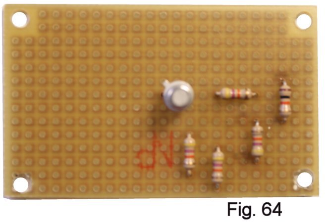
All of the resistors are formed for four holes, so the leads are simply bent
close to the body. They can be installed in any order, and heat-sinking is
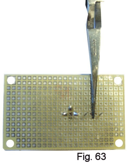
not needed. An easy way to begin is with R8, which goes from index P-7 to
S-7. Hold the component in place with soldering tweezers, solder, and trim
leads (Fig. 63). Then add R4, R5, R10 and R11. Continue with the rest of the resistors on the
left side, R1, R2, R3
and R6 (Fig. 65). |
|
|
|
   |
|
|
|
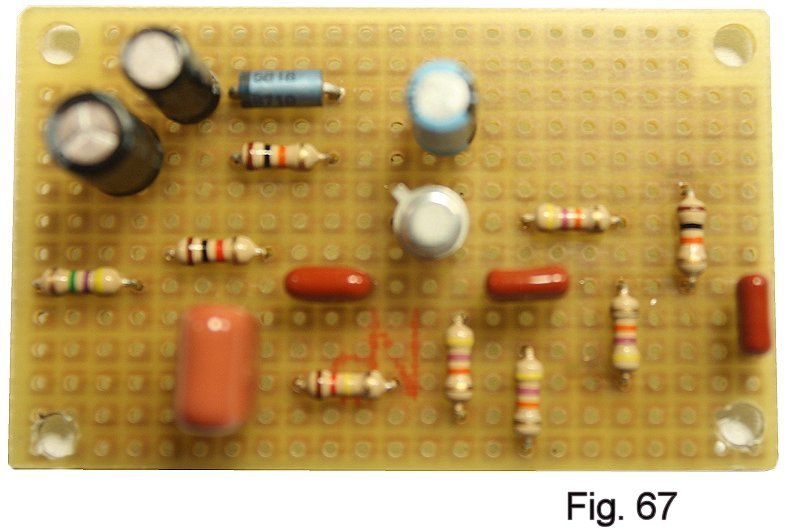
OK, capacitors. C2, C3, C6 and C7 are polyester-metal film and have no
polarity, so they can be inserted either way. C3 may span three to five
holes depending on the make (Fig. 66). Again, use soldering tweezers to hold the
component in place while soldering. When adding the electrolytic capacitors,
C1, C4 and C5, observe polarity! The same caution applies to installing
diode D1 (Fig. 67). The LED will go in last during assembly. The board is now stuffed and we can begin to wire. |
|
|
|
  |
|
|
|
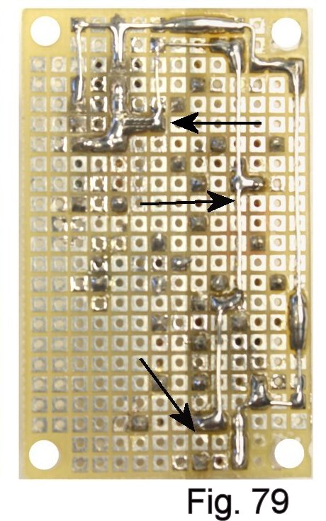
Let's do the ground bus first, starting at index E-3, the negative side of
capacitor C4. (I'll show you later when we do terminations how to make the
connection to E-1.) Cut a length of bare wire about 2" long. Using soldering
tweezers to hold the wire, butt it up to index E-3 as shown and solder (Fig.
68). Using the chain-nose plier, make a sharp right angle bend down column
A. Cut the wire so that it just butts against index A-9 where resistor R-1
terminates. "Tack" the run in the corner where you made the bend. Hold down
the run with
tweezers and solder to join at index A-9 (Fig. 69).
Before you continue the run, use the soldering iron to remove the
remaining pad material around the mounting holes that were added earlier.
Butt the remaining wire against index A-9 and solder to join it to the pad
(Fig. 70).
Now make two right-angle bends, one at A-12 and one at C-12. Tack the run
at C-12 and cut off at C-14 (Fig. 71). |
|
|
|
|
   
|
|
|
|
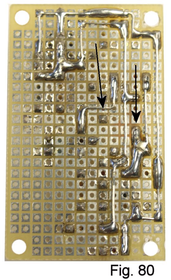
Now extend this part of the ground bus to R5 (Fig. 72) and end it at C7
(Fig. 73). A little bit
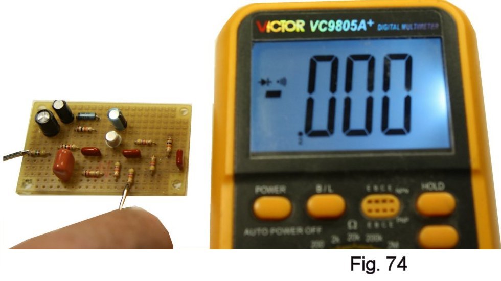
of soldering connects resistor R10 to index T-12 (also Fig. 73), and let's stop and do a test.
According to the layout, we should have a connection all the way from the
negative side of C4 to one side of C7, right? We can't easily test
continuity from C4, but we can absolutely test from R1 to R5 (Fig. 74). Got a good
connection? If not, check your soldering. If all is OK, mark off the section
you have tested on the layout, the schem, or both (Fig. 75). |
|
|
|
|
|
|
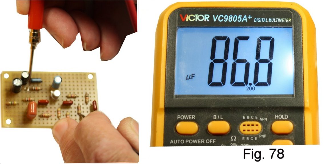
If your meter has a capacitance scale (as many do), it's possible to test
continuity through a section that contains a capacitor. Let's get the + side
of capacitor
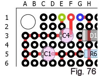
C1 connected to diode D1 (Fig. 76) and I'll show you what I mean. You can see in the
pic where I have made the connection between the + side of C1, R6 and the
negative side of the diode. I have also made the connection between the negative
side of C1 and the ground bus. So it would make sense that if I measure
capacitance from the negative (bar) side of D1 to any point on the ground
bus, I should see about 100 mf. I see 86.8 here, and that's within the normal 20%
tolerance for an electrolytic, so I'm good. Use this technique wherever
convenient to help ensure correct wiring! |
|
|
   |
|
|
|
Next, lay down the positive supply bus starting at index E-5. Tack it at B-7
and B-11 for mechanical stability. Then pick up
one side of resistor R3 and end on one side of resistor R11 at index U-9.
Join one side of resistor R5 to one side of resistor R3 and pick up one side
of resistor R4. Then do a run to one side of capacitor C3. The opposite side
of C3 terminates at the Emitter of the transistor, and that's a good point
from which to do the capacitance/continuity test if you can. |
|
   |
|
|
|
Here is a list of the remaining connections in the order in which I did them
with some notes where I thought they would be helpful: |
|
|
- R1 to R2. Avoid getting solder on pad D-8 when making this connection,
because we will add a termination there later.
- R2 to C2
- Index H-1 to index J-7. Leave index G-7 clear for now. After we do the
terminations later, you can test continuity from the Emitter of Q1 to this
point.
- Base of Q1, one side of capacitor C2 and one side of resistor R4
- Collector of Q1 to positive side of C5 and join to R6
- Negative side of C5 to capacitor C6 and pick up one side of resistor
R8
- Leave index P-1 open for a termination. Start a run from just below
index P-1 to one side of capacitor C6 and one side of resistor R10
- Leave index R-1 open for a termination. Start a run from just below
index R-1 to one side of resistor R8 and one side of capacitor C7
- Leave index S-3 open to add the + side of the LED later. Start a run
from just below index S-3 to one side of resistor R11
- Leave index T-3 open to add the - side of the LED later. Start a run
from just to the right of index T-3 to just short of index W-4
The board is wired, and we can prepare to connect to off-board
components. |
|
|
|
Terminations |
|
|
|
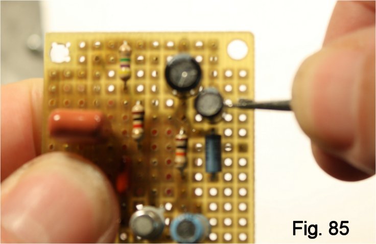
Too many DIY builds will have you insert leads in the holes (Fig. 82), connect to
pots, jacks and switches and then stuff the board in the
enclosure. I find these methods tacky and won't teach that way. One "right"
way to terminate to an off-board component is to insert a push-in terminal
(I call these "flea clips") into the appropriate hole and solder on the
underside of of the board. Then you can mount the board on standoffs and
wire to the terminals. Start with the hole at index E-1. Enlarge the hole
slightly by "working" it with an awl or straight pick (Fig. 83). Squeeze the bottom of
the terminal slightly with the chain-nose plier (Fig. 84), insert in the hole, and
push down in the top slot--firmly and steadily--with the side of a small
screwdriver to seat the terminal (Fig. 85). |
|
|
    |
|
|
|
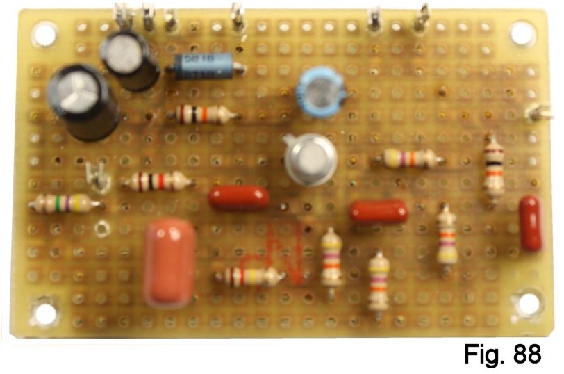
In many cases, you can immediately solder the terminal in place on the
bottom. I wanted to bridge the one-pad gap to index E-3, so I made use of
the fact that the terminal has a hole in the bottom for inserting wire. I
re-opened the flange with a pick to enlarge the hole, slipped a bit of wire
in (Fig. 86), soldered and trimmed (Fig. 87). Done. The remaining terminals are installed at
indexes F-1, G-1, J-1, P-1, R-1, D-8 and W-4 (Fig. 88). The board is finished, and the
next step is to prepare the enclosure.
|
|
|
|
   |
|
|
If you bought a kit, the enclosure is already drilled. If not, and you are
rolling-your-own in a 125-B box, you can download from
here a page of
drilling templates. Never used these? Here is a quick review of my methods:
- With a good, sharp scissor, cut out the top template.
- Attach a couple of pieces of double-sided clear or masking tape to the
box, and carefully center the template to the cover.
- In the same way, attach the templates for the sides, being careful to
get the holes for the jacks in the correct locations to the right and left
of the switch.
- Use a scribe or scratch-awl to put a small dent at the center mark of
the hole for the stomp switch (Fig. 89).
- If you use standard twist drills, bore a 1/8" pilot hole, enlarge it with a ¼" drill, and then use a tapered reamer to slowly bring the hole to its final size.
- Follow the same procedure for the other three holes on the top, and then the holes on the sides.
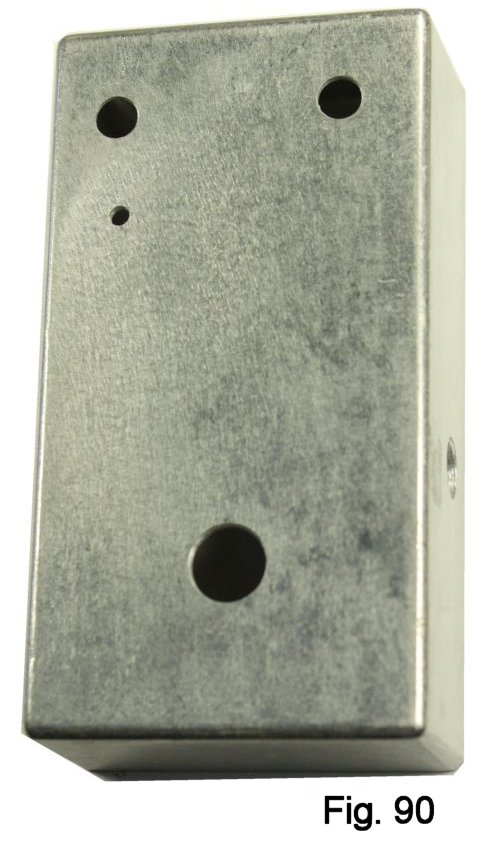
- De-burr all of the holes with a small, round file. Remove all of the
templates and tape, and you should have the result shown (Fig. 90).
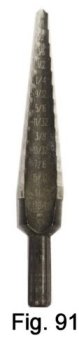
Note: Many people like using a step drill (the common trade name is Unibit) rather than separate drills, because it does a quick, clean job of boring any size hole from 1/8" to 1/2"
(Fig. 91). |
|
|
|
   |
|
|
|
Before installing standoffs for mounting the board, do any painting or
decorating that you want to. There are so many choices and methods for how
to do this that they really need a separate treatment. You can find lots of
discussion and useful infomation by searching past threads on the Forum.
Once the enclosure is decorated, you want to keep it from accidentally being
dinged while you work. Put a soft cloth down on your work surface to protect
the face, and Move Slowly, especially when you have a tool in your hands
(long experience!). |
|
|
|
I have noted that I insist on using standoffs of some kind to anchor the
board rather than supporting it on a few wires and stuffing the case with
styrofoam. There are numerous metal and/or plastic hardware items that can
be used to secure a board, and the choice depends on a mixture of mechanical
needs and cost. Plastic standoffs (Fig. 92) won't fly here because the
board butts against the walls of the box. Better, in this case, to use epoxy
cement to attach aluminum studs (Fig. 93) to the case. Done right, this results in a
gig-worthy and reliable build. The ones shown are hex-shape, 3/8" long and
tapped for a 4-40 screw, Keystone #1892. The kit includes four of them and
four screws. First job is to mark the areas in the enclosure that need to
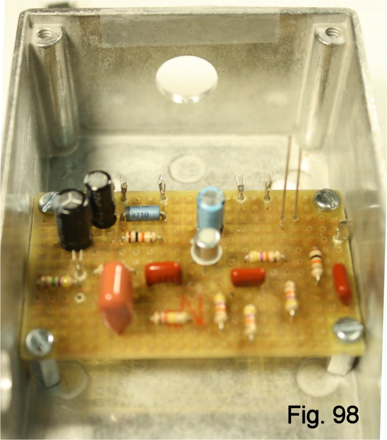
be prepped. Set the LED in place temporarily at indexes S-3 and T-3, and
lower the board into place (Fig. 94). The LED should be exactly vertical its holes.
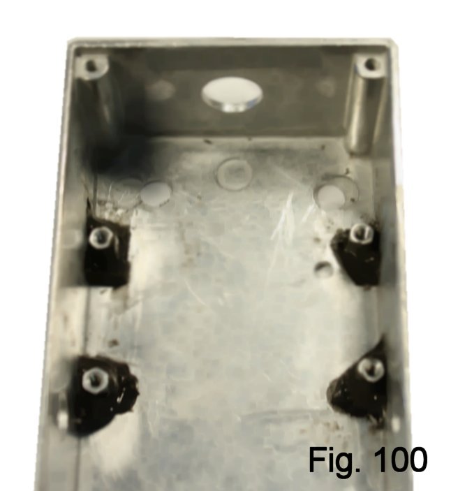
Now mark the locations of the mounting holes with a pick or scribe (Fig. 95). This
indicates the areas where the surface of the box will need to be cleaned. |
|
|
   
|
|
|
|
With coarse sandpaper (80 or 100 grit), roughen the marked areas on the
floor and on the walls above the marks. Then scrub thoroughly with a Q-tip
wetted with acetone. Screw the studs to the board (finger-tight only) and
prep them the same way that you did the box--roughen and clean up with
acetone. Again place the LED temporarily and set the board in place. Take
care not to touch any of the surfaces you prepped. |
|
|
   |
|
|
|
Mix a small volume of quick-setting epoxy cement (I like J-B Weld). Apply a
small amount of the epoxy to the accessible areas at the base and sides of
the studs. WAIT a few hours until the epoxy has cured thoroughly and then
remove the screws. Take out the screws, remove the board and beef up
the epoxy all around each stud, taking care to avoid the LED hole.. NB: If you don't like having to go through
all of this (and I really don't, even though I know it's necessary), check
out the Bare Box #1; the studs are cast into the side walls and all of the gluing
is eliminated. Prepare the LED for mounting by cutting two 3/8"-long
pieces of vinyl tubing (saved scraps from insulated wire work for this) and
sliding on to the leads. The shorter lead is negative. Using the chain-nose
plier, bend the leads at right-angles to each other. Cut down the ends and
solder in place on the bottom of the board, being careful to observe
polarity. When you assemble now, the LED will drop into its hole. |
|
|
     |
|
|
I know that you were wondering if we would ever get here...We are ready to wire!
Install the stomp switch and jacks, orienting all as shown with hardware on
finger-tight.
- Wire from the Ring contact of the stereo jack to the center-pin
contact of the power jack. The center-pin also gets the negative lead of
the battery snap. The positive battery snap lead goes to the switched
contact. Refer to figure 4 if you need to.
- Create a ground run that connects the sleeve contacts of the jacks.
The sleeve of the stereo jack gets a connection that will terminate on the
board later. The sleeve of the mono jack gets a connection that will
terminate on the stomp switch later.
- The board can be installed.
- Wire the stomp switch: Solder a jumper between contact #1 and contact
#4. Use different colors of wire to make tracing easier. Rout the wire
from contact #6 under the board. This will terminate later on the tone
pot.
|
|
|
|
|
|
|
Solder short different-colored leads to the terminals of the (5K) boost
potentiometer and mount the control with hardware finger-tight. Take care to
solder each terminal to its correct termination on the board. The ground
connection from the jacks and the CCW terminal of the potentiometer both
terminate at index E-1. Install the tone potentiometer in the same way.
The lead from the stomp switch goes to the center terminal. Make the short
connection to the power jack from the + power input of the board. |
|
|
|
|
|
|
The pedal is ready to test. Connect a battery and your gear and see if the
controls work. I built exactly what you see here, so you should have action
if everything is as posted. |
|
To complete the job:
- Tighten the hardware on the controls and jacks
- Secure the lid
- Stuff a small piece of foam padding over the battery
- Install the battery cover
- Install knobs
- Install rubber feet
|
|
|
|
Troubleshooting |
|
|
|
The first rule to keep in mind is that projects like this are
all-or-nothing. If EVERYTHING is correct, the build works; if ONE thing is
wrong, it doesn't. But you have something going for you: I built from the
drawings shown here, and you can rely on them. Use them as your bible, and
you'll find out what's wrong.
To start troubleshooting, make clean copies of both the schematic and the
layout drawing. Use a highlighter to mark off connections as you check them.
Go over the off-board connections first and verify that the connections to
power, jacks and switch are correct. If those look good, you have to
verify the interconnections. Very Carefully, disassemble the pedal and lift
the board and controls out of the enclosure. Use the continuity setting of your multimeter
to make sure that you actually have a connection between every point in the
layout that is supposed to be connected, and that nothing is shorted. Found
a bug? Time to do repairs.
You can also use the low-voltage scale of your meter to sniff out
problems. With your guitar plugged in (necessary so that the battery
circuit is complete), hang the negative lead on the sleeve of the input
jack. You should see roughly the following voltages on Q1: Collector 5.48
volts, Base 2.39 volts, Emitter 1.77 volts. If any of your readings are off
these by more than 10%, you probably have a wiring error. |
|
|
|
Enjoy your new pedal! More builds employing this basic two-knob platform are under development. Comments and suggestions are welcome at
smallbearelec@ix.netcom.com. |
|
|
|
A Parts List |
|
|
|
Presuming that you have all the parts in the breadboard kit, here's what's
needed for the generic build: |
|
|
|
1 |
Enclosure 125-B |
0306B |
|
1 |
3PDT stomp switch |
0200 |
|
2 |
Knobs for 1/4" shaft |
0825C |
|
4 |
Studs |
8009 |
|
4 |
4-40 Screw x 1/4" |
8003 |
|
1 |
Pad-per-hole perfboard |
0355 |
|
8 |
Push-in Terminals |
0400C |
|
1 |
Bare tinned wire |
0509 |
|
1 |
Hookup Wire |
|
A kit that includes everything on this list is available as SKU 0016D. |